GENERAL CONDITIONS OF USE PRIVACY POLICY
This privacy policy is given in observance of the normative in force regarding the protection of personal data and, in particular, pursuant to EU Regulation 2016/679 (GDPR) and legislative decree 196/2003 (Code regarding the protection of personal data, so-called “Privacy Code”) with reference to processing the personal data of visitors to the website www.iqonic-h2020.eu . The website is owned and managed by CRIT S.r.l This privacy policy is only issued for this website and any other domains, websites and landing pages owned by CRIT S.r.l. which may be consulted by users through internal links and/or websites consulted directly by the user which are attributable to the ownership of CRIT S.r.l. This privacy policy contains important information about personal data that are collected when visiting this Website as a registered or unregistered user and it describes the ways in which such data are used.
This document contains important information about the following:
1) DATA CONTROLLER
2) PURPOSE AND METHOD OF PROCESSING
3) THE WAY IN WHICH DATA ARE CONVEYED AND CONSEQUENCES OF REFUSAL
4) THE PLACE IN WHICH DATA ARE PROCESSED
5) TYPE OF PROCESSED DATA/SPECIFIC PROCESSING
6) RETENTION PERIOD
7) RECIPIENTS/CATEGORIES OF RECIPIENTS OF PERSONAL DATA
8) RIGHTS OF THE DATA SUBJECTS
9) RIGHT OF REVOCATION AND OPPOSITION
10) PROTECTING THE PRIVACY OF MINORS
11) SAFETY AND CONFIDENTIALITY OF PERSONAL DATA
12) UPDATES OF THIS EXPLANATORY DOCUMENT - COMMUNICATIONS
- DATA CONTROLLER
For the purposes of this Privacy policy and the processing of data described herein, we specify that CRIT S.r.l. – VAT - IT02648490361 – having its registered office at Via Confine 2310 tel. 059/776865, info@iqonic-h2020.eu, is the data controller (as defined in Regulation (EU) 2016/679) of the collected data. For any comments or questions regarding this Privacy policy and to speak with the local contact person assigned to managing queries regarding data processing, it is also possible to contact the Company’s customer service at the email address info@iqonic-h2020.eu or by calling: 059/776865.
- PURPOSES AND METHODS OF PROCESSING
After having consulted this website and having used one or more services, data concerning identified or identifiable natural persons may be processed. Such personal data, where acquired and always in observance of the normative in force, shall be processed solely for the following purposes:
a) Strictly associated purposes instrumental for allowing access and use of the website, its functions, requested services and services provided by the Company, amongst which, by way of example: replying to requests for information from a user;
b) Send information about the services, professional activities, advertising and commercial activities, products and activities of CRIT S.r.l., in order to perform market or statistical surveys and to send information about new properties for sale;
c) Personalisation and improvement of the tools and functions in the www.iqonic-h2020.eu Website;
d) In order to comply with the obligations provided by law and the European normative and measures of the competent Authorities;
e) For reasons of an operational and managerial nature pertaining to the Company internally and concerning the offered services and/or products;
In the case of explicit and optional manifestation of consent, the data collected for the purposes pursuant to paragraph a) shall also be processed for the purposes of direct marketing by the Data Controller, especially for sending informatory, commercial or advertising material about the services and/or products offered by the Company, also via email, sms, fax and other instant, or not, messaging tools which may also operate on third party platforms. The data shall be processed lawfully and correctly and only used for the purposes pursuant to the paragraphs hereabove. Processing shall take place using tools suited to guaranteeing the security and confidentiality of the personal data and may take place using paper based means and/or automated and computerised tools aimed at storing, managing and transmitting such data.
- THE WAY IN WHICH THE DATA ARE PROVIDED AND CONSEQUENCES OF REFUSAL
The provision of personal data is mandatory exclusively for the purposes pursuant to art. 2, paragraph a) so as to allow the use of the website and services associated and requested by the user, possibly subject to disclosure for each service issued as established by law. Your refusal shall make the use of such services impossible. However it shall be possible to consult the website without providing any personal data although some functions shall not be available and some services cannot be supplied. The provision of the data and giving consent for the related processing for the purposes pursuant to art. 2, paragraph b), is optional: without explicit consent such services shall not be provided. However, there are no other consequences. If you do not wish to give your consent for such purposes you may equally use the website and services for the purposes pursuant to art. 2, paragraph a). In other words, the consequences of a refusal to respond or give consent are always explicit and connected to each provided service. For example, in the event of refusing the related processing, the consultation of the website and all its functions (in the case of cookies), receiving the newsletter (in the case of the newsletter service) or receipt of advertising material (in the case of art. 2 paragraph b) may be impeded. The user is thereby informed in an appropriate manner for each concrete case, but may, in any case, consult the website even if he/she denies consent for processing personal data where requested: in this event such functions and features of the website could be disabled.
- THE PLACE IN WHICH DATA ARE PROCESSED
Processing associated to the web services pursuant to this website is performed at the seat of Studio Three-Sixtieth, Via Cà Dè Lolli nr.105, Marano sul Panaro, 41054, Modena – Italy , without prejudice to explicit exceptions, and it is only overseen by the technical staff of the Company expressly assigned to processing. The website hosting service is provided by Studio Three-Sixtieth,. at the servers owned by the latter kept within the farm of Register S.p.A. in Italy, which guarantees the Data Controller, inasmuch as of its competence, the observance of the normative in force on the matter of processing personal data.
- TYPE OF PROCESSED DATA/SPECIFIC PROCESSING
Different types of personal data can be processed depending on the provided service, as specified in this article.
5.1. Navigation data
The computer systems and software procedures for the operation of this website acquire some personal data during the course of their normal running, the transmission of which is implicit when navigating websites. This information is not collected in order to be associated with identified interests: nonetheless given its nature it could allow users to be identified through processing and association with data held by third parties. The latter include IP addresses or the domain names of the computers used by users connecting to the website, URL addresses of the requested resources, the time of the request, the method used to submit the request to the server, the size of the file obtained in response, the number code indicating the status of the response given by the server and other parameters related to the operating system and the platform utilised by the user. The data pursuant to the above are only used in order to obtain anonymous statistical information about the use of the site and in order to control the correct operation thereof: they are deleted immediately after processing. The data could be used for ascertaining responsibility in the case of hypothetical cyber crimes to the damage of the website: without prejudice to such possibility, at the current time data on web contact do not persist for more than seven days. See section 5.4 below in relation to cookies.
5.2.1. Data voluntarily provided by the user (communications)
Optional, explicit and voluntary provision of communications through contact forms on the website or emails to the addresses given in this website lead to the subsequent acquisition of the data provided by the sender, including their email address and consent to receive any messages in response to their requests. The personal data thus provided are only used to satisfy or respond to the transmitted requests and are only communicated to third parties in the case that this is necessary for such purpose. Specific explanatory documents drawn up for special services on demand shall be shown in the related pages of the website.
5.2.2. Data voluntarily provided by the user (to receive communications for the purposes of marketing and/or commercial promotion)
Each data subject may voluntarily provide their personal data to CRIT S.r.l. in order to receive commercial or promotional communications, howsoever called, with digital and paper based communications. In the sole case in which the email details are given by the data subject in the context of selling a product or service can the email address thus provided be used for the direct sale of other similar products or services, pursuant to EU Regulation 2016/679 (GDPR) and legislative decree 196/2003 (Code on the matter of the protection of personal data, so-called “Privacy Code”), without the necessity for express and prior consent. In any case, the data subject is reminded in every communication that they can revoke consent at any time and without formality. The data are deleted upon request of the data subject.
- RETENTION PERIOD
The data provided shall be retained for the periods prescribed by legal norms and, in any case, for the time strictly necessary to pursue the activities for which they were collected and/or until revocation of the consent given for the purposes pursuant to art. 2, paragraph b).
Nonetheless, the collected data shall be retained for no longer than twenty-four months for the marketing purposes pursuant to art. 2 paragraph b) (without prejudice to any amendments and/or supplements to the normative of reference on the matter of protecting personal data which shall be expressly communicated therein).
Personal data shall be protected from the risks of destruction, access by unauthorised parties and use for purposes other than those for which consent was given.
- CATEGORIES OF RECIPIENTS OF PERSONAL DATA
The data acquired via web or in any case originating from web services, may be communicated to technological and instrumental partners of which the Data Controller avails to issue the services requested by users/visitors, provided that in observance of the purposes indicated in art. 2.
The data collected for the foregoing purposes may also be communicated to companies that are associated or belong to the same corporate group of the Data Controller, as well as subjects authorised for such purpose by legal and European regulatory provisions.
- RIGHTS OF THE DATA SUBJECT
The data subject is the identified or identifiable natural person to whom the personal data subject matter of processing refer.
We inform you that in your capacity as data subject, you are granted the right to access the data concerning you at any time, processed by the Data Controller (right of access) so that you may verify that they are correct and verify the lawfulness of the completed processing. You may also exercise all the rights granted by the normative in force, national and European, regarding the protection of personal data (by legislative decree 196/2003 and by EU regulation no. 2016/679 as amended): in particular, you may request correction and updating of incorrect or imprecise data at any time, you may also restrict processing and request the cancellation of data (right to be forgotten), and also lodge a complaint to the Supervisory Authority for the protection of personal data.
With reference to the personal data processed using automated means, lastly, you are granted the right to receive the data concerning you in a structured and commonly used format, as well as sending them, where applicable, to another data controller (right to data portability).
So as to allow CRIT S.r.l to best serve its users, the latter are invited to update their personal data on a regular basis.
- RIGHT OF REVOCATION AND OBJECTION
Each data subject is also granted the right to revoke conferred consent at any time, without prejudice to the lawfulness of the processing carried out by the Data Controller before such revocation. Data subjects are also granted the possibility to object to processing data concerning them when this has been carried out for direct marketing purposes as pursuant to art. 2, paragraph b; in this case your data shall no longer be subjected to processing for such purposes (right to object).
- PROTECTING THE PRIVACY OF MINORS
This Website addresses the generic public, nonetheless its services are intended for persons who are 18 years old or older. CRIT S.r.l. does not request, collect, use or divulge personal data provided by persons younger than 18 on a deliberate basis. If CRIT S.r.l. realises that it has personally collected data from a minor it shall erase them.
If a user is not of the required age they are kindly asked not to register and to ask an adult (namely their parents or guardian) to carry out the necessary procedures.
We specify that pursuant to art. 8 of the European Regulation, where article 6, paragraph 1, letter a) applies, as regards the direct offer of information services to minors, the processing of the minor’s personal data is lawful when the minor is at least 16 years old.
- SECURITY AND CONFIDENTIALITY OF PERSONAL DATA
CRIT S.r.l. implemented measures suited to protecting the user’s personal data from accidental loss and unauthorised access, use, modification and disclosure. Password checks, firewall technology and other technological and procedure based security measures are used in the management of this website. Despite the fact that CRIT S.r.l. implemented the aforementioned security measures for the Website, the user should be aware that it is not possible to guarantee 100% security. Therefore the user provides their personal data at their own risk and to the maximum extent permitted by the law in force, CRIT S.r.l. shall not be liable in any way whatsoever for their disclosure due to errors, omissions or unauthorised actions by third parties during or after their transmission to the latter. CRIT S.r.l. advises the user to periodically update software to protect the transmission of data on networks (antivirus software for example) and to check that the electronic communication service provider has adopted means suited to safe transmission of data on the networks (firewalls and junk mail filters for example); to keep their user name and password to access the account confidential and not divulge them; and to periodically change their password.
In the unlikely event that CRIT S.r.l. deems that the security of the user’s personal data in its possession or under its control has been or could have been jeopardised, it shall inform the user thereof according to the procedures provided by the law in force and using the method prescribed therein (in providing CRIT S.r.l. with their email address, the user accepts receipt of such communications in electronic format via such email address).
- UPDATE OF THIS EXPLANATORY DOCUMENT - COMMUNICATIONS
At its discretion CRIT S.r.l. reserves the right to change, amend, supplement or delete part of this Privacy policy at any time, publishing the reviewed version thereof on this page of the Website and updating the last amendment date shown below. The user is responsible for looking at the Privacy policy again from time to time so as to keep abreast of any amendments brought thereto. In some cases CRIT S.r.l. may issue further communications concerning relevant changes to this Privacy policy, publishing a notice on the home page of this Website or, in the case of registered users, sending a notification email or inserting a notice on the page of their account. By accepting such reviewed Privacy policy by clicking on the “accept” button in the notification email or communication published on the account page (where provided in order to comply with the laws in force), using or sending information to the Website after publication of the reviewed Privacy policy, the user accepts such reviewed Privacy policy. Following the amendments where provided under the normative in force, the user’s data shall not be the subject matter of processing without explicit consent from the user.

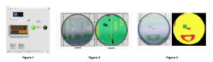 Figure 1: LabVIEW program and GUI that assess the waveguide quality of semiconductor laser devices and display the results. Figure 2: Example of image annotation (COCO Annotator) by CORE Innovation. Figure 3: Image of a wafer revealing the top grating and the corresponding defect detection result.
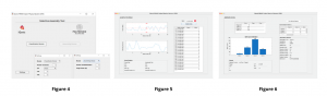 Figure 4: CPS main Screen. Figure 5: CPS classification Module. Figure 6: CPS assembling Module.
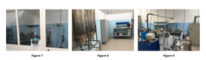 Figure 7: FILAR shop floor with ultrasonic drilling station into optomechanical area. Figure 8: FILAR shop floor with laser marking station into optomechanical area.Figure 9: FILAR shop floor with lapping and polishing stations into optomechanical area.

0 Comments